New "Electronic Glue" Promises Less-Expensive Semiconductors

A vial of nanocrystals in solution, which serve as
“electronic glue” for semiconductor-based technologies.

University
of Chicago Postdoctoral Scholar Maksym Kovalenko
(left) working with nanocrystals in a glovebox in the laboratory of Dmitri
Talapin, assistant professor in Chemistry. Working in the environmentally
controlled conditions of the glovebox permits researchers to perform chemical
procedures not possible under room conditions.
Photos by Dan Dry.
Photos by Dan Dry.
Semiconductors have served as choice materials for many electronic and optical devices because of their physical properties. Commercial solar cells, computer chips and other semiconductor technologies typically use large semiconductor crystals, but these are expensive and can make large-scale applications such as rooftop solar-energy collectors prohibitive.
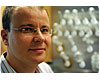
Dmitri Talapin is an assistant professor in Chemistry at the
University of Chicago.
The “electronic glue” developed in Dmitri Talapin’s laboratory at the University of Chicago solves the ligand problem. The team describes in the journal Science how substituting the insulating organic molecules with novel inorganic molecules dramatically increases the electronic coupling between nanocrystals. The University of Chicago licensed the underlying technology for thermoelectric applications to Evident Technologies in February.
Sources
Citation: “Colloidal Nanocrystals with Molecular Metal Chalcogenide Surface Ligands,” Maksym V. Kovalendo, Department of Chemistry, University of Chicago; Marcus Scheele, Molecular Foundry, Lawrence Berkeley National Laboratory; and Dmitri V. Talapin, Department of Chemistry, University of Chicago, and Center for Nanoscale Materials, Argonne National Laboratory, Science, June 12, 2009.Funding sources: American Chemical Society Petroleum Research Fund, The Chicago Energy Initiative, U.S. Department of Energy and Evident Technologies Inc.
Looking for a reprint of this article?
From high-res PDFs to custom plaques, order your copy today!


