
Electronic components that contain a die require a path by which excess heat can be removed from the component package. In low-voltage plastic-encapsulated microcircuits, the heat may simply travel by conduction through the die attach and the die paddle for dissipation through the bottom of the package. In higher-voltage integrated circuit (IC) packages and in larger items such as insulated-gate bipolar transistor (IGBT) modules, a separate metal heat sink may be adhesively bonded to the package. The heat sink promotes conduction and prevents the temperature of the die from rising to a point where the circuitry on the die will fail. The bonding agent holding the heat sink in place may be solder, epoxy or another material. The heat sink is usually on the bottom of the component package, although some flip chips have a heat sink on the top side of the package.
In products where system longevity matters, it is worthwhile to inspect the bonding of the heat sink to the component in order to avoid components that have internal structural defects that will compromise the dissipation of heat from the die. The most frequent defects are gaps of some type in the bond holding the heat sink in place. The gaps may be voids (trapped air bubbles), non-bonds (where a factor such a surface contamination prevents adhesion of the bonding material) or cracks. The terms disbond and delamination may also be used for these defects.
Each of these gaps is an efficient blocker of heat flow and promotes higher temperatures in the die. Even in the absence of gaps, heat flow can be compromised by a non-planar element in the layered structure of the package. This condition is seen in IGBT modules, where the ceramic raft may be tilted or warped.
Inspecting Images for Defects
Pre-mounting inspection for all of these defects is carried out by an acoustic micro-imaging (AMI) tool*. These tools use ultrasound to produce acoustic images of internal features, including gaps, in the components. The acoustic images permit users to separate, accept and reject components. Because many of the gaps are extremely thin, X-ray typically cannot image them. Ultrasound, by contrast, depends for imaging on the interface between the gap (air or another gas) and a solid.
For acoustic inspection, the components are placed on the instrument’s stage with the heat sink upward (except for IGBT modules, which will be explained later). An ultrasonic transducer moves back and forth a few to several mm above the surface of the heat sink, and is coupled to the heat sink surface by a column of water that moves along with the transducer.
The AMI tool’s transducer can move at a speed above 1 m/s. While moving, it performs the following routine several thousand times per second: a pulse of ultrasound is launched into the transducer, the ultrasound is reflected by one or more material interfaces within the sample, and the arrival time (depth) and amplitude of each returning echo is recorded.
After launch from the transducer, a pulse may encounter three different situations:
- When the pulse is traveling through homogeneous material, no echo is returned.
- When the pulse encounters the interface between two solid materials (such as epoxy and silicon), a portion of the ultrasound is reflected back to the transducer and recorded, while another portion crosses the interface and travels deeper into the sample. Solid-to-solid interfaces produce medium-amplitude echoes. They are displayed in the raw acoustic image as gray pixels ranging from light gray (high amplitude signal) to dark (low amplitude signal).
- When the pulse encounters the interface between a solid material and a gas such as air, virtually all of the ultrasound is reflected back to the transducer. These are the highest amplitude return echo signals, displayed as bright white pixels in the raw acoustic image. They identify the gap-type defects that block heat flow. Virtually all of the ultrasound is reflected, even if the gap is as thin as 0.02 microns, far smaller than gaps that can be detected by X-ray.
Echoes are actually returned from any depth where the pulse encounters a material interface, but the echo signals that are used to make the acoustic image are usually collected only from a defined depth of interest; for example, the adhesive material bonding the heat sink to the layer above the bond material. To avoid overlapping of features, echoes from other depths are not recorded.
Acoustic Imaging
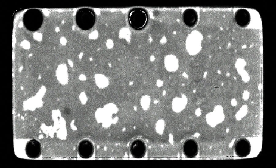
Figure 1 shows an acoustic image made by scanning the surface of the metal heat sink on a large module. Bolts hold the heat sink to the layer above. The AMI tool’s transducer scanned the entire area of the heat sink. Return echo signals were collected from the depth of the solder.
Over most of the area, the echoes produce a medium gray color, meaning that the amplitude of reflections from the heat sink-to-solder interface and from the solder-to-next layer interface is neither very high nor very low. But scattered throughout the solder are variously sized high-amplitude white features that are probably voids. They are large enough and numerous enough to block a substantial amount of heat.
Defects that block heat flow are especially critical in IGBT modules because these modules (used as switches in heavy-duty applications such as subway motors and mine drilling equipment) deal with high voltage and power. Modules are designed to permit maximum thermal dissipation downward toward a metal heat sink. A typical path passes from the die through the die attach, the ceramic raft and the solder to the heat sink.
IGBT modules were originally not being imaged by an AMI tool because of the water column that couples the transducer to the surface of the sample. Voltage levels are so high in these modules that even the slightest residue left by water could become a leakage path and result in failure of the module in operation. A few years ago, the first inverted AMI system was developed: both the transducer and the water column are inverted and placed underneath the stage on which the IGBT module rests. The transducer scans the bottom surface of the heat sink, thereby keeping the top surface dry. Return echo signals can be received from any material interface at the depth of the heat sink, the ceramic raft, the die attach material, or the die itself.
The ultrasound pulsed into an IGBT module is usually gated on a specific depth of interest, meaning that only echoes from within that depth are used to make the acoustic image. The depth of greatest interest is often the solder bonding the heat sink to the ceramic raft above it.
If experience has shown that a particular IGBT module fails only because of defects in the solder, the assembler may inspect the modules by imaging only the solder depth. IGBT modules can be inspected either before or after overmolding of the module, because the heat sink is left exposed. If defects are found before encapsulation, the module can be reworked.
Ultrasonic Pulse Measuring
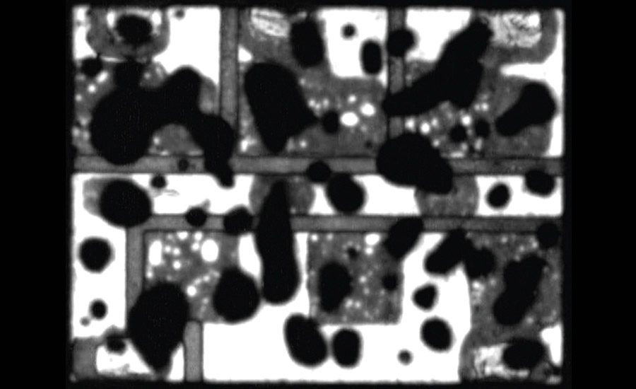
Return echo signals are not always gated on the solder. In Figure 2, gating was limited to the die attach near the top of the module. Echoes from lower depths were ignored. In the gated die attach depth, several die are visible, as are numerous voids in the die attach. The voids are white because of the solid-to-air interface. The voids and the die are largely obscured by numerous black features, which are acoustic shadows. Ultrasound that is pulsed to the die attach layer returns to the transducer as echoes. On the way to the transducer, it encounters large voids in the solder. The voids locally reflect the returning ultrasound back toward the die and create acoustic shadows corresponding to the shape of each void.
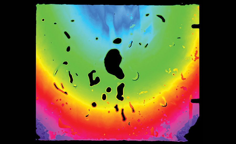
The ultrasonic pulse can be used to measure properties other than the amplitude of a return echo. For example, in the time difference mode, the arrival time of an echo is measured to determine the depth from which it was reflected. Instead of assigning a color to the echo’s amplitude, the color is assigned to its depth. In the acoustic image, items at different depths will be displayed in different colors.
The time difference mode was used to make Figure 3. One of the problems with IGBT modules is that the ceramic raft soldered to the heat sink can become tilted or warped. Both of these conditions can lead to mechanical stresses within the die because heat distribution from the die is not uniform. In Figure 3, the AMI tool was used to map the topography of a warped raft. Since the heat sink itself is not warped, acoustic imaging also measures the thickness of the solder at each of the thousands of x-y coordinates at which an echo was received. The dark blue regions at the top center mark the lowest points on the raft, and hence the greatest solder thickness.
The raft gradually rises through green, yellow, red and magenta regions until, at the bottom left and right corners, it becomes black. Black indicates that the raft is virtually in contact with the heat sink. The scattered black features in the image are voids. Most of the voids are black because, like the corners of the raft, they are very close to the heat sink. Those closer to the raft have the color assigned to their depth. Despite its internal flaws, the external appearance of this IGBT module would not suggest that its heat-dissipating ability had been compromised.
Nondestructive acoustic inspection of heat sinks can be performed by a laboratory C-SAM tool for small quantities or on automated in-line tools for larger quantities. The percent of the bond area filled with voids can be calculated automatically. Inspection can use any of numerous additional acoustic imaging modes to diagnose the defects and keep defective components and modules out of production. ASI
For more information, visit www.sonoscan.com.


