
In the late 2000s, researchers at Technical Research Center of Finland (VTT) invented a new optical method to image 3D microtopography of surfaces at sub-micron resolution. This method, called line confocal imaging (LCI), is based on capturing a continuous line of light reflections in visible spectrum from more than 2,000 lateral surface points simultaneously.
Line confocal sensors—and scanners based on them—are used in the imaging of surfaces, transparent materials, and multi-layered structures in various metrology and inspection applications on discrete parts, assemblies, webs, and other continuous products. Imaging results can be used to characterize a product’s form, surface topography, roughness, flatness, thickness and 3D volume. The LCI method also has a tomographic functionality, which enables the capture of 3D structures under transparent layers, as well as the simultaneous acquisition of 2D gray-scale (intensity) images from single or multiple surfaces with a large depth of focus covering the sensor’s entire z range, up to 5.50 mm.
Line Confocal Imaging
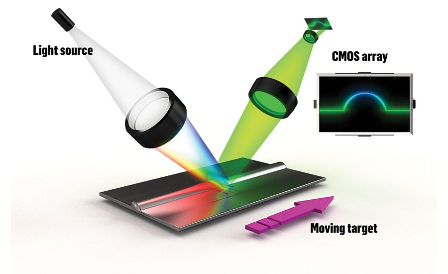
Each LCI sensor has two front lenses—one for its transmitter and another for the receiver. Figure 1 depicts an LCI sensor’s imaging principle. The sensor’s transmitter has a light source that emits white light containing all visible wavelengths. A complex optical assembly separates the light into wavelengths and focuses a horizontal line of each color at a different distance from the sensor, forming a focal plane.
Depending on the vertical position of the imaged surface within the plane, corresponding wavelengths from 2,048 lateral measurement points are reflected back to the sensor’s receiver simultaneously. The receiver’s spectral camera captures wavelength and intensity information from each point and forms related height profiles and intensity lines. When the surface moves in front of the sensor, a 3D point cloud and a 2D gray-scale image are generated from the scanned surface line by line. The resulting data can be processed, analyzed and reported with various 3D surface analysis and image processing software packages.
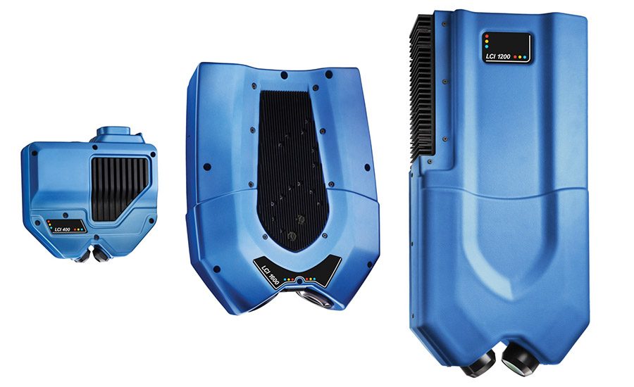
Three sensor models are available to suit the imaged material, surface type and resolution requirements. The sensor with highest resolution offers height (z) resolution of 100 nm and z range of 1 mm. The next model up in size has z resolution of 0.55 µm and z range of 2.80 mm, while the largest model has z resolution of 0.98 µm and z range of
5.50 mm. Lateral resolution in measurement line direction (x) varies from 2.20 to 8.00 µm, depending on the sensor model. Y resolution depends on the line spacing and motion speed of the surface in the application. The length of the sensors’ measurement line ranges from 4.50 to 16.40 mm.
The sensors can be integrated in both off-line and real-time in-production metrology systems, as they can operate at the speed of up to approximately 5,000 lines/sec. This results in a data acquisition rate of over 10 million 3D surface points per second. Data from multiple interfaces in multilayered structures and 2D intensity image data, also potentially from several layers within the scanned area, further increases this number.
Benefits of Line Confocal Imaging
LCI sensors and systems work well in applications that require high-speed imaging of challenging materials at sub-micron resolution. Scanning an area that would require tens of minutes for traditional 3D imaging methods, such as point confocal or interferometric technologies, can be now completed within a few seconds.
Transparent materials and products with highly reflective or mirror-like surfaces are ideal for LCI. The sensors’ large numerical aperture and high tolerance for surface angle allow for imaging of steep slopes and glossy curved surfaces. LCI does not suffer from speckle noise; this enables surface imaging at much higher resolution than laser triangulation sensors.
The quality of raw image data produced by LCI sensors is excellent and rarely needs filtering or other manipulation of any kind. Since the sensors capture 2,048 measurement points simultaneously, vibration of the imaged surface or the sensor itself seldom causes issues; relative point height positions within the measurement profile line remain unaffected.
Adhesives and Sealants Applications
Most LCI sensors and systems are currently used in research and development and quality control of discrete parts, assemblies, and continuous products. LCI can be used to image transparent, translucent and opaque structural and pressure-sensitive adhesives, sealants, and other materials in liquid, paste, and solid forms.
Shape, size, cross-sectional area, height, width, volume, surface roughness and position of glue dots and lines can be measured with LCI sensors. The technology works equally well on sealants and other dispensed materials. Materials can be characterized with LCI sensors both in laboratory and production conditions in real time.
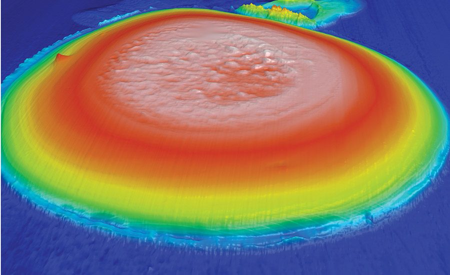
LCI technology works well in challenging applications, such as imaging transparent glue dots on transparent or mirror-like surfaces. Figure 2 (p. 24) shows a 3D view of an approximately 85 µm high bead of transparent cyanoacrylate glue on a glossy transparent glass substrate. The bead was scanned with an LCI sensor. Figure 3 (p. 24) depicts a 2D top view of the same bead with its automatically calculated volume and height values.
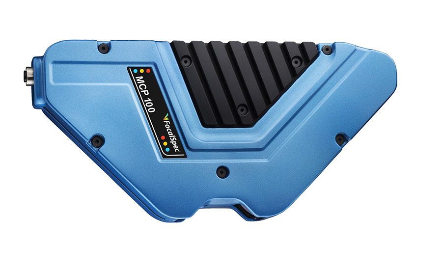
In addition to topographic and tomographic 3D imaging, LCI sensors can also be used to measure thickness of transparent layers and coatings. For in-process thickness measurement applications where 3D imaging is not required, a dedicated monochromatic dual-point IR sensor MCP100 can be used. It measures thickness, distance and surface angle of transparent and semi-transparent layers and coatings at the speed of up to 10,000 measurements per second at resolution of 50 nanometers.
For more information, phone (770) 713-0837, email juha.saily@focalspec.com or visit www.focalspec.com.


