Polymer Progress
New
polymer could improve semiconductor manufacturing, packaging.
 Researchers at Rensselaer Polytechnic Institute, Troy, NY, and Polyset
Co., Mechanicville, NY, have developed an inexpensive,
quick-drying polymer that could lead to dramatic cost savings and efficiency
gains in semiconductor manufacturing and computer chip packaging.
Researchers at Rensselaer Polytechnic Institute, Troy, NY, and Polyset
Co., Mechanicville, NY, have developed an inexpensive,
quick-drying polymer that could lead to dramatic cost savings and efficiency
gains in semiconductor manufacturing and computer chip packaging.
Along with allowing enhanced performance and cost savings for conventional photolithography processes, the new material, called polyset epoxy siloxane (PES), should also enable a new generation of lower-cost, on-chip nanoimprinting lithography technology, according to the researchers.
“With this new material, chip manufacturers will be able to trim several steps from their production and packaging processes, and in turn realize a cost savings,” said Toh-Ming Lu, the R.P. Baker Distinguished Professor of Physics at Rensselaer, who oversaw the study. “PES is cheaper and more reliable.”
Lu’s research was published in the Journal of Vacuum Science and Technology B.
The widely adopted technique of photolithography involves using a mix of light and chemicals to generate intricate micro- and nano-scale patterns on tiny areas of silicon. As part of the process, a thin polymer film called a redistribution layer, which is crucial to the effectiveness of the device, is deposited onto the silicon wafer in order to ease the signal propagation delay and to protect the chip from different environmental and mechanical factors.
The new PES material developed by Lu’s group and Polyset Co. is one such thin polymer film, and it offers several advantages over the incumbent materials typically used in semiconductor manufacturing. In addition, the new PES material can also be used as a thin polymer film for ultraviolet on-chip nanoimprinting lithography technology, which is still in the early phases of development. The consistency of using PES in conventional technology, and then continuing to use PES while academia and industry test and gradually migrate to the next generation of devices, should help ease the transition, Lu said.
“Having the ability to use one material - our new PES - for both photolithography and imprint will be very attractive to manufacturers,” Lu said. “At its core, our project is basic research, but it also has important industry implications. It’s very exciting.”
Manufacturers today typically use benzocyclobutene and polyimide as polymers for redistribution layers, because of their low water absorption, thermal stability, low curing temperature, low thermal expansion, low dielectric constant, and low leakage current. Lu said PES offers significant advantages to these materials, particularly in the areas of cure temperature and water uptake.
 PES cures - or dries and hardens - at 165°C, about 35%
cooler than the other two materials. The need for less heat should translate
directly into lower overhead costs for manufacturers, Lu said. Another
advantage of PES is its low water uptake rate of less than 0.2%, less than the
other materials. In addition, PES adheres well to copper and can easily be made
less brittle, if needed. All of these attributes make PES a promising candidate
for redistribution layer application and UV imprint lithography.
PES cures - or dries and hardens - at 165°C, about 35%
cooler than the other two materials. The need for less heat should translate
directly into lower overhead costs for manufacturers, Lu said. Another
advantage of PES is its low water uptake rate of less than 0.2%, less than the
other materials. In addition, PES adheres well to copper and can easily be made
less brittle, if needed. All of these attributes make PES a promising candidate
for redistribution layer application and UV imprint lithography.
“The results demonstrate that PES is feasible to be used as UV-curable resist for both the redistribution application for electronic packaging and micro/nano imprint lithography,” said Rensselaer Research Associate Pei-I Wang, co-author of the paper.
Along with photolithography and on-chip nanoimprinting lithography, PES holds the potential for applications in other optical devices, flat-panel display, biotechnology devices, and microelectromechanical systems, Wang said.
In addition to Lu and Wang, co-authors on the paper include Rensselaer materials science and engineering professor Omkaram Nalamasu, who is also chief technical officer of Applied Materials Inc. in Santa Clara, CA; Rajat Ghoshal and Ram Ghoshal of Polyset Co. Inc. in Mechanicville, NY; Charles Schaper of Transfer Devices Inc. in Santa Clara, CA; and Andrew Li of Applied Materials.
The project was funded through the New York State Foundation for Science, Technology and Innovation.
Lu’s research was conducted as part of Rensselaer’s Center for Integrated Electronics. The center’s multidisciplinary team of more than 50 faculty researchers and 100 graduate students aims to advance the role of electronic devices in our everyday lives by accelerating the production of the next generation of micro- and nanoelectronic devices and systems. The Center’s mission is to build integrated top-down and bottom-up nanostructures, devices, and systems for information, biological, and broadband communication applications. Major activities include pioneering research into gigascale interconnects, 3-D interconnect structures, materials properties and process modeling, wideband gap semiconductors and devices, terahertz devices and imaging systems, power electronic devices and systems, and biochips.
For more information on Lu’s research and Rensselaer’s Center for Integrated Electronics, visit www.rpi.edu/~lut/ and www.rpi.edu/dept/cie .
For more information on the new PES materials, visit www.polyset.com.
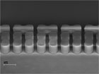
Researchers from Rensselaer Polytechnic Institute’s
Department of Physics and Center for Integrated Electronics have developed an
inexpensive, quick-drying polymer that could lead to dramatic cost savings and
efficiency gains in semiconductor manufacturing and computer-chip packaging. In
this scanning electron microscope image of the new PES polymer in a
photolithography application, the straight side walls indicate the material’s
good photodefinition characteristics.
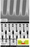
A scanning electron microscope image showing the imprints of
trenches and dual-damascene structures realized using PES in the newly
developed molecular-transfer lithography process, indicating the potential of
PES for microchip applications.
Along with allowing enhanced performance and cost savings for conventional photolithography processes, the new material, called polyset epoxy siloxane (PES), should also enable a new generation of lower-cost, on-chip nanoimprinting lithography technology, according to the researchers.
“With this new material, chip manufacturers will be able to trim several steps from their production and packaging processes, and in turn realize a cost savings,” said Toh-Ming Lu, the R.P. Baker Distinguished Professor of Physics at Rensselaer, who oversaw the study. “PES is cheaper and more reliable.”
Lu’s research was published in the Journal of Vacuum Science and Technology B.
The widely adopted technique of photolithography involves using a mix of light and chemicals to generate intricate micro- and nano-scale patterns on tiny areas of silicon. As part of the process, a thin polymer film called a redistribution layer, which is crucial to the effectiveness of the device, is deposited onto the silicon wafer in order to ease the signal propagation delay and to protect the chip from different environmental and mechanical factors.
The new PES material developed by Lu’s group and Polyset Co. is one such thin polymer film, and it offers several advantages over the incumbent materials typically used in semiconductor manufacturing. In addition, the new PES material can also be used as a thin polymer film for ultraviolet on-chip nanoimprinting lithography technology, which is still in the early phases of development. The consistency of using PES in conventional technology, and then continuing to use PES while academia and industry test and gradually migrate to the next generation of devices, should help ease the transition, Lu said.
“Having the ability to use one material - our new PES - for both photolithography and imprint will be very attractive to manufacturers,” Lu said. “At its core, our project is basic research, but it also has important industry implications. It’s very exciting.”
Manufacturers today typically use benzocyclobutene and polyimide as polymers for redistribution layers, because of their low water absorption, thermal stability, low curing temperature, low thermal expansion, low dielectric constant, and low leakage current. Lu said PES offers significant advantages to these materials, particularly in the areas of cure temperature and water uptake.
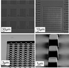
A series of scanning electron microscope images of the new
PES polymer in a UV-imprint lithography application. The well-defined pattern indicates
the material’s potential for use in next-generation chipmaking techniques.
Along with allowing enhanced performance and cost savings for conventional
photolithography processes, PES should also enable a new generation of
lower-cost, on-chip nanoimprinting lithography technology.
“The results demonstrate that PES is feasible to be used as UV-curable resist for both the redistribution application for electronic packaging and micro/nano imprint lithography,” said Rensselaer Research Associate Pei-I Wang, co-author of the paper.
Along with photolithography and on-chip nanoimprinting lithography, PES holds the potential for applications in other optical devices, flat-panel display, biotechnology devices, and microelectromechanical systems, Wang said.
In addition to Lu and Wang, co-authors on the paper include Rensselaer materials science and engineering professor Omkaram Nalamasu, who is also chief technical officer of Applied Materials Inc. in Santa Clara, CA; Rajat Ghoshal and Ram Ghoshal of Polyset Co. Inc. in Mechanicville, NY; Charles Schaper of Transfer Devices Inc. in Santa Clara, CA; and Andrew Li of Applied Materials.
The project was funded through the New York State Foundation for Science, Technology and Innovation.
Lu’s research was conducted as part of Rensselaer’s Center for Integrated Electronics. The center’s multidisciplinary team of more than 50 faculty researchers and 100 graduate students aims to advance the role of electronic devices in our everyday lives by accelerating the production of the next generation of micro- and nanoelectronic devices and systems. The Center’s mission is to build integrated top-down and bottom-up nanostructures, devices, and systems for information, biological, and broadband communication applications. Major activities include pioneering research into gigascale interconnects, 3-D interconnect structures, materials properties and process modeling, wideband gap semiconductors and devices, terahertz devices and imaging systems, power electronic devices and systems, and biochips.
About Rensselaer
Rensselaer Polytechnic Institute, founded in 1824, is the nation’s oldest technological university. The university offers bachelor’s, master’s and doctoral degrees in engineering, the sciences, information technology, architecture, management, and humanities and social sciences. Institute programs serve undergraduates, graduate students and working professionals around the world. Rensselaer faculty are known for pre-eminence in research conducted in a range of fields, with particular emphasis in biotechnology, nanotechnology, information technology, and the media arts and technology. The Institute is well known for its success in the transfer of technology from the laboratory to the marketplace so that new discoveries and inventions benefit human life, protect the environment and strengthen economic development.About Polyset
Polyset Co. is a technology-driven materials company with a philosophy of designing resin systems around needs. It is a market leader within product areas of focus, and has been a leader in urethane adhesive systems and corrosion-resistant primers for many years. Much of its new product development is based on new proprietary advanced materials, catalysts and associated formulations that deliver functionality. In these endeavors, it focuses on wafer-level manufacturing and interconnect assembly, incorporating both electronic and optical packaging material. In addition, the company has developed novel 100%-solid coating formulations for the coil-coating industry that allows for the elimination of solvent-based coating. Polyset provides contract manufacturing services for resins, prepolymers, adhesives and related components for diverse companies, including Fortune 50 corporations.For more information on Lu’s research and Rensselaer’s Center for Integrated Electronics, visit www.rpi.edu/~lut/ and www.rpi.edu/dept/cie .
For more information on the new PES materials, visit www.polyset.com.
Links
Looking for a reprint of this article?
From high-res PDFs to custom plaques, order your copy today!


