The Emergence of Benzocyclobutene in Bonding Electronics

BCB has been used in the fabrication of flat-panel displays.
Photo courtesy of www.newscom.com.
Photo courtesy of www.newscom.com.
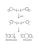
Figure 1. BCB polymerization pathways
Developed in the 1980s, BCB has been a commercial technology since the 1990s, used initially in the fabrication of radio-frequency integrated circuits and flat-panel displays.1 Since then, its application across electronics has broadened, and one element of that success has been its precisely controllable and readily monitored thermal curing process.
This particular level of control arises from BCB’s two-step polymerization reaction, which starts with a thermally activated opening of the dihydrocyclobutene ring. The resulting highly reactive o-quinodimethane diene usually reacts via a Diels-Alder reaction with a dienophile to form a tri-substituted tetrahydronaphthalene, however it can react with itself to give the dimer, l,2,5,6-dibenzocyclooctadiene, or polymerize in a similar manner to a 1,3-diene to give poly(o-xylene).
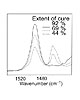
Figure 2. Monitoring BCB cure by IR spectroscopy
Commercially, BCB is most commonly available as a partly prepolymerized resin based on divinylsiloxane bisbenzocyclobutene (DVS-BCB). This molecule is a BCB dimer, where the two monomers are crosslinked with a structure that contains both vinyl dienophile and siloxane adhesion-promoting functionality.
The extent of the curing reaction can be monitored by infrared spectroscopy. A specific absorbance band at 1500 cm-1 corresponds to a vibration of the tetrahydronaphthalene polymerization product, and its intensity grows as the reaction continues. There is also an absorbance at 1475 cm-1 from the four-membered cyclobutene reactant group that disappears as it is consumed.2 In DVS-BCB, these peaks may be normalized to a 1254 cm-1 absorbance, arising from silicon-bonded carbons that are unaffected by the polymerization.3
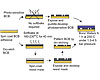
Figure 3. BCB Processing
Applying BCB to Semiconductor Wafers
Exploiting the two-stage approach means that cure can be obtained in a matter of minutes at 300°C, although an hour is needed at the conventional cure temperature of 250°C. Above 42% conversion, the polymer becomes a soluble gel, while above 70% the material becomes a glassy amorphous solid.Once cured, BCB does not melt and reflow with temperature, but with a 52 ppm/°C coefficient of thermal expansion it does expand.4 It also expands in the course of curing at temperature, with the chip assembly then subjected to strain from contraction as it cools. If the assembly is then reheated at a higher temperature than used for curing, the BCB will exert expansion stresses on the chip. This is a challenge, as 400°C annealing steps are common in electronics manufacturing, but stresses can be reduced by minimizing the thickness of the BCB layer.5
When used with semiconductor wafers BCB is typically applied using spin-coating to µm thicknesses, and sometimes utilizes adhesion promoters for higher bond strength.6
When being processed to an exact shape for specific chip designs, it is typically partially cured to ensure resistance to subsequent manipulation, in particular plasma-etching and the removal of materials used in photolithographic masking. However, the degree of polymerization should not be too high, since this limits adhesive properties later in the process.
A layer of photosensitive resist material is then spin-coated on top, exposed to light to introduce a pattern, and developed. Plasma-based reactive ion etching may subsequently be used to etch the pattern in the photomask onto the BCB coating. The remaining resist is then chemically removed, using acetone, for example.
Photosensitive BCB is available and simplifies the process, which starts with exposure to UV light, brief heating, and treatment with a developing chemical. So-called “puddle-development” sees the chemical sit on a slowly rotating wafer that spins it off before the wafer is rinsed and spun dry. The unwanted BCB can then be removed with a short plasma treatment.
Wafers are usually bonded using commercially available bonders that bring them together under vacuum and heat them to perform the final curing of BCB.
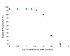
Figure
4. Planarization effectiveness of a 2-µ-thick BCB film for
different chip dimensions.
Desirable Properties
The unconventional polymerization chemistry of BCB is desirable to the electronic industry because it produces a material with both an extremely low moisture uptake capacity and a low dielectric constant.Moisture absorption is a problem in many other bonding materials used in electronics due to the fact that water can cause corrosion and has a dielectric constant of 70 when polarized. BCB typically only absorbs up to 0.12% by weight of water, and has a low dielectric constant of 2.64.
A low dielectric constant helps to reduce the buildup of charges known as parasitic capacitances in chip manufacture, which can improve the efficiency of electronic devices such as micro-electro-mechanical systems and radio-frequency transistors. Efficiency is boosted further as BCB’s resistivity at 1019 Ocm makes it more effective as an insulating layer, thus reducing unwanted current leakage.7
Continued miniaturization in ultra-large-scale integration has increased the need for the benefits of BCB in interlevel dielectrics, the principal use of BCB other than the direct wafer bonding discussed above. In addition to providing good electronic properties in chip manufacturing, it produces highly planar layers, which are important, as subsequent layers that are formed above may lie irregularly on uneven layers. DVS-BCB polymer reflows during the early stage of cure, redistributing material and eliminating the need for repeated processing to fill gaps.
The overriding trend in the electronics industry is one of miniaturization, which in turn often demands the integration of different functions. In the past, BCB could be accused of only being an appropriate technology for niche microelectronic applications, but its ability to bring together different chip materials is likely to prove ever more useful in the future.
Looking for a reprint of this article?
From high-res PDFs to custom plaques, order your copy today!


