Get the Lead out
Legislation in Europe (RoHS) requires the implementation of Pb-free products by June of 2006. Electronic Industry groups have evaluated several of these lead-free materials and have chosen the Sn/Ag/Cu alloy as a short to mid-term solution. The typical alloy composition is Sn96.5Ag3.0Cu0.5 (called SAC305) and reflows at a temperature of 217
Pb-Free Implementation and Concerns
What are the concerns when implementing a Pb-free soldering process? The first and most critical concern is component integrity. Components will have to withstand higher processing temperatures for which most are not specified. Therefore, in order to implement a Pb-free solder paste into production, components must first be evaluated and qualified to survive higher process temperatures.
A second concern with implementing a Pb-free soldering process is the qualification of a Pb-free solder paste. There are two major concerns with the implementation of a Pb-free solder paste: 1) solder paste print performance and 2) reflow characteristics. The solder paste should behave no differently than a SnPb solder paste and be capable of handling a very large process window. Ideally, an assembly manufacturer would like to have a solder paste that is capable of reflowing at very low temperatures (230
Pb-Free Solder Paste Evaluation
In order to implement a Pb-free solder paste into production, the paste must have performance characteristics similar to Sn/Pb solder pastes. Therefore, some of the critical parameters that must be studied during the evaluation phase are: print quality, stencil life, tackiness and wetting.
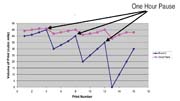
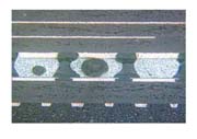
Print quality is critical to any manufacturing process, and the Pb-free process is no exception. To evaluate the printing characteristics of each paste, volumetric measurement capability of the paste depositions should be available and the measurement system must be capable of repeatable measurements for the finest apertures used in production. First, the print parameters of the Pb-free solder paste should be optimized to determine the critical parameters for the solder paste, such as print speed or pressure. Once the parameters have been optimized, a print-deposition study comparing the Pb-free solder paste to the SnPb paste performance may be completed. The next print performance test to complete is the paste stencil life experiment. The paste must perform over the course of a manufacturing day, and, in typical manufacturing processes, equipment downtimes of one to two hours are not uncommon. Therefore, the ability of a solder paste to accommodate these downtimes and print acceptably is critical for the implementation of a Pb-free soldering process. Figure 1 compares the print volumes between solder pastes that have acceptable and unacceptable "response to pause."
Reflow Profile Process Window
Phase 1 - Bare Board Wetting
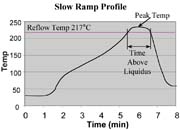
To evaluate the reflow process window of a solder paste, various peak temperatures and liquidus times should be tested. A minimum of three reflow profiles should be evaluated: a low peak temperature of 230
The reflow performance of a Pb-free solder paste must also be evaluated in soldering performance on standard components. A typical production or test board that contains standard components can be used. The test boards should be reflowed again using the various reflow profiles (low, medium and high peak temperatures).
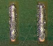
The following cross-sections exhibit very good component soldering wetting results when using a Pb-free solder paste with a wide process window. Figure 5 shows the cross-section of a component at the low reflow peak of 230
Determining Product Readiness
After evaluating the various solder pastes, as well as the ability to solder components at the required higher temperatures, a product must be designed to undergo the Pb-free transition. The preferred product should have a minimal thermal gradient across the entire circuit board so that a lower process temperature can be implemented. The most critical stage of Pb-free implementation is selection and approval of components. The components must be capable of handling higher reflow temperatures without issues. The required reflow temperatures must be stated in the component specification. If a component cannot function at increased process temperatures, then either a new supplier must be chosen or in-house analysis must be completed to verify the capability of the component.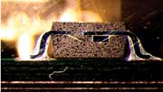
Production Evaluation and Implementation
The following is an example of a product that was implemented into a Pb-free soldering process. During the pilot and product qualification stages of the Pb-free soldering process, several manufacturing issues were revealed that needed to be resolved prior to full-scale production. Typical problems included the following.- Reduced wetting or spreading
- Increase in tombstone components
- Increase in BGA voiding on Sn/Pb bumps
- Component integrity compromised during soldering
- Component MSL rating
- Soldering to gold-plated contacts or connectors
The sections below detail the solutions found for these manufacturing product issues.

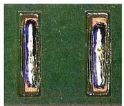
The implementation of a Pb-free soldering process is different than the standard Sn/Pb process. The most obvious observed difference in the soldering is the visual wetting difference. The Pb-free solder will not wet completely out to the solder pads. This may only be a cosmetic difference, but operators must be trained to inspect for the difference. If reduced wetting is believed to be a problem - exemplified by exposed copper on the PCB, for example - then an increase in stencil aperture size may be required to resolve the issue.

One of the biggest problems found in the initial pilot stages was the increase in small chip component tombstoning. Initially, it was thought that the reduced wetting of the Pb-free (SAC) alloy would bring about an improvement in the tombstone performance, but this was not the case. Compared to Sn/Pb alloys, Pb-free SAC alloys have higher surface tension and thus a stronger pulling force on the chip component. Figure 9 shows an example of a typical tombstone failure.
Appropriate chip component pad design is therefore critical for optimum soldering performance. It was noted that a reduction of overall pad length assisted in improving the tombstone performance. In addition, a reduction in paste deposition may also be considered in order to optimize soldering performance.
Figure 9 shows that a via-in-pad design was utilized. This was also noted to increase the tombstone occurrence and will be eliminated in future designs. Consider the use of HDI technology for designs that require this application.
In addition, the reflow profile was found to have an impact on tombstone performance. The critical part of the profile was observed to be the ramp, or soak, portion of the heating cycle. Therefore, the optimization of the profile is necessary to improve the soldering performance of small chip capacitors and resistors.
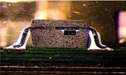
The next major problem found in implementing a Pb-free solder paste was the compatibility between Sn/Pb solder bumps and BGAs or CSPs. The problem discovered was very large solder voids in the solder joint. Figure 10 shows an example of a typical BGA solder joint formation using a Pb-free paste and Sn/Pb (lower melting) ball.
The problem is relatively easy to understand. The Sn/Pb ball on the BGA component reflows prior to the higher-temperature (Pb-free) solder paste wetting. The typical solder paste makeup for the Pb-free solder paste contains solvents and activators that are active and volatilize at temperatures higher than 180
Higher reflow process temperatures have an effect on component integrity. The following are a few observations noted during the pilot builds.
Higher process temperatures can discolor or degrade the appearance of some components. This may be purely cosmetic, but needs to be understood and evaluated for the product.
Some components have sensitivity to absorbing moisture. These components are presently controlled in standard production environments by placing them in dry boxes or baking them if they are exposed to long stretches of humidity. The process temperature will also have an effect on component performance. The higher the peak reflow temperature, the greater the possibility of damaging a component. Therefore, experimental analysis must be completed to evaluate the effect on a component's ability to perform. In summation, greater care must be taken with all components that are sensitive to moisture when evaluating the ability to solder at Pb-free temperatures.
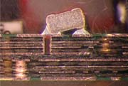
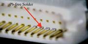
This was an issue that did not reveal itself until late in the product pilot stages. It is known that the Pb-free (SAC) solder alloys exhibit less wetting and spreading of the solder on the pad or component, but this was found not to be the case with gold-plated components, such as contacts or connectors. The high temperature Pb-free solder has an affinity to wet with gold due to its higher tin content. In some cases, it was found that Pb-free solder would wet all the way up a component lead termination and intrude into the package. Figure 11 shows the Pb-free solder extending all the way through the package and onto the lead. This example caused the lead to fail to mate with the corresponding female connector, which resulted in a defect. The resolution to this problem was to modify the paste-printing apertures in order to minimize the wetting of the Pb-free solder paste on the gold-plated lead.
Conclusion
It is possible to implement a Pb-free soldering process on today's electronic products, but it is not a drop-in fit compared to the Sn/Pb process. Following are key points to observe.- A robust Pb-free solder paste must first be qualified for a Pb-free process. The solder paste must have a large process window and be capable of uniform performance over a range of temperatures, preferably lower temperatures, but also mid- and high-temperatures.
- Components must be carefully chosen and qualified to perform at higher process temperatures.
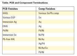
- PCB finishes and component terminations should be considered prior to initial product assembly.
- Product design must be well thought out and evaluated for a Pb-free process. Modifications to standard pad geometries may be required to optimize the Pb-free soldering process.
- The product must undergo accelerated life testing to evaluate the Pb-free solder joint strength and reliability as they compare to standard Sn/Pb solder joints.
Product design and component selections have a significant effect on the introduction of a Pb-free soldering process. Several manufacturers have implemented Pb-free solder paste. The majority of the products produced at present are only Pb-reduced, since not all component terminations are 100% Pb-free. To implement a Pb-free manufacturing solution, all manufacturing processes must be characterized and optimized for peak performance. This is because the Pb-free manufacturing process window is much tighter than the standard Sn/Pb process we are accustomed to today.
For more information on lead-free solder paste, contact Indium, phone (800) 4-INDIUM or (315) 853-4900; or visit http://www.indium.com.
References
1. Butterfield, A.; Visintainer, V.; Goudarzi, V. "Lead Free Solder Flux Vehicle Selection Process," SMTA International 2000 proceedings.2. Lee, N.C.; Huang, Benhlih. "Prospect of Lead Free Alternatives for Reflow Soldering."
3. Bradley, E. "Overview of No-Lead Solder Issues," NEMI meeting, Anaheim, February 23, 1999.
Looking for a reprint of this article?
From high-res PDFs to custom plaques, order your copy today!


