Tips and Services for Potting-Optimized Component Design
Designers of electronic components can avoid faulty potting by considering these best practices and communicating with relevant stakeholders early in a product’s design phase.
With regard to potting, the design of electronic assemblies and components has a significant impact on economical and sustainable production. Key aspects in this respect are pottability, material use, cycle times, quality, and the process technology needed. Optimized, bubble-free potting contributes greatly to the function and longevity of products. This white paper presents potting tips to consider for best practices during the design and development phases.
Key Aspects
1. What requirements do engineering and design have to meet?
Designers have great responsibility when designing a product. There are various issues that need to be considered in electronic component development, and any conflicts have to be resolved. An example of this are the aspects surrounding production and potting. If engineers and product designers take these into account during component development there will be multiple benefits (Fig. 1). To achieve the best possible results there needs to be a comprehensive interchange between the system planning, production, and after-sales departments so that experience with previous products can be leveraged. The involvement of system and material suppliers is also useful in order not to miss any new, economical design options. If all these aspects are incorporated in the component design, the overall result will also be impressive in terms of total cost of ownership.
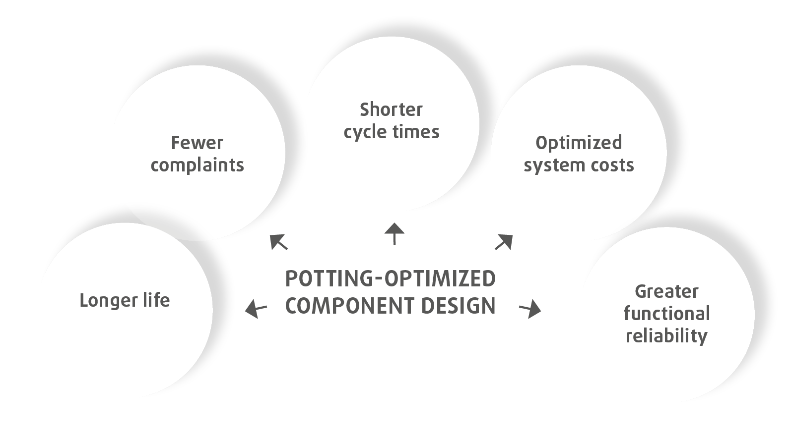
Figure 1: The benefits of potting-optimized component design can have a significant effect on total cost of ownership.
2. What does potting-optimized component design involve?
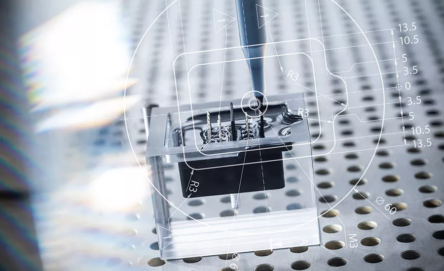
Potting-optimized component design involves displacing air during the potting process and facilitating such displacement. This will prevent the presence of bubbles in the potting material, which sometimes have serious consequences for the correct operation of the product.
3. Why should bubbles be avoided?
Air pockets in the potting material have adverse effects. Depending on the product, they may reduce service life or even cause complete failure. In some circumstances they may contribute to thermal loads and therefore stresses inside the component and even cracks in the outer skin. Air bubbles have poor thermal conductivity, reduce insulation, and therefore reduce the dielectric strength of components, for example. They also encourage corrosion.
4. How can bubbles in the potting material be prevented?
There are a number of rules to be met, as described below. When designing a component, it is important to consider the potting process — specifically the direction of flow of the potting material and therefore the direction in which air is displaced.
5. What about design security?
Errors made in component design can be corrected later only at great expense in terms of time and money, if at all. Design security results from adherence to the potting rules and early dialog with all the various departments in the company and with material and system suppliers. If existing experience is not sufficient for potting-optimized component design or if new materials are being used, testing under production conditions in a technology center will help. This will ensure that all the questions are clarified at an early stage and within a reasonable timeframe. This creates security for an economical and sustainable potting process and the required product quality.
6. Why is potting-optimized component design sustainable?
Potting-optimized component design has high sustainability potential. Minimal waste, reduced material use, and shorter cycle times are not only economic but also provide eco-friendly advantages that are becoming increasingly important.
Constructive Tips
Component miniaturization, more complex shapes, increasing security-relevant use of electronic components, sustainable use of materials — all these things define the requirements for absolutely bubble-free potting. Following the tips below represents an important step forward. It does not matter whether the potting is for filling, sealing, or impregnating electronic components. The direction of flow of the potting material and therefore the free displacement of the air is always the crucial element.
*Click the image for greater detail
1. Avoid horizontal surfaces
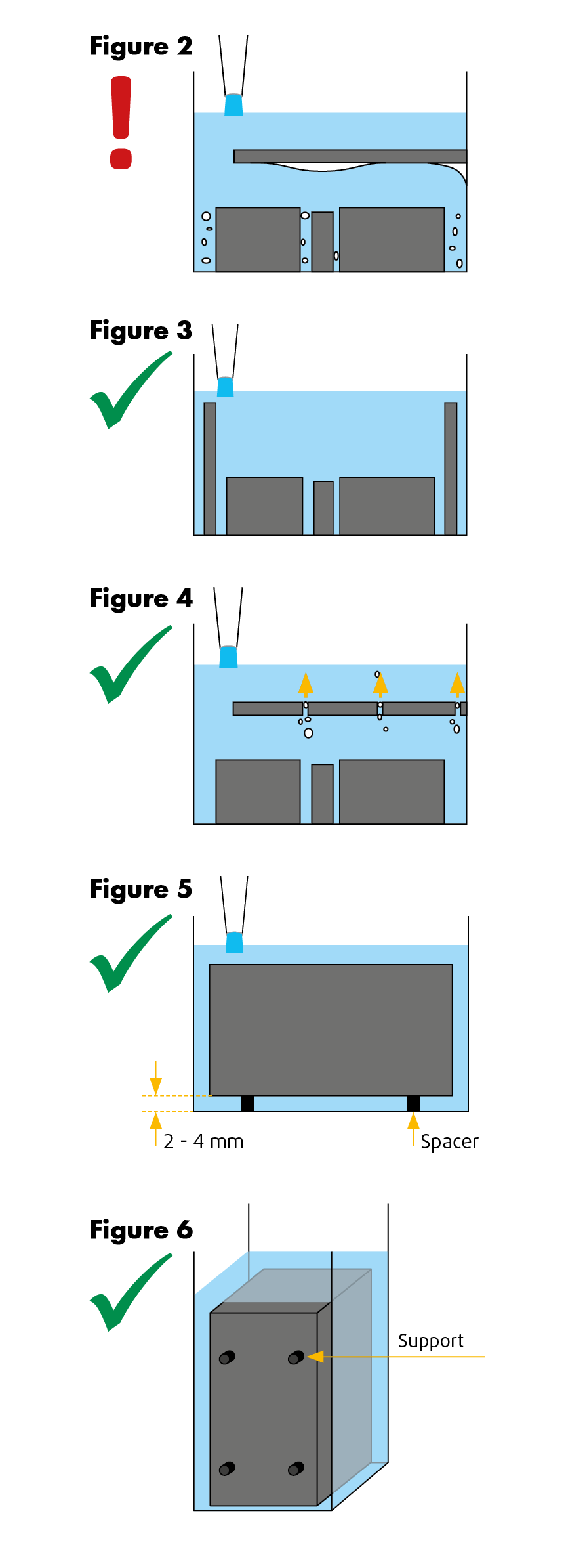
Components embedded horizontally (Fig. 2) are obstacles to rising air bubbles. They may prevent the underlying contacts from being completely enclosed by the potting compound because of the formation of air bubbles.
2. Provide space for air to escape
The larger the number of components the smaller the potting spaces. A large amount of air is stubbornly trapped in the fine gaps of windings, such as those of ignition coils. If this only gradually escapes during potting under atmospheric pressure or not at all, it is advisable to pot the components under vacuum. There are two design measures that will facilitate the escape of air: If components with large horizontal surfaces are arranged vertically (Fig. 3) the air can escape more easily. If the overall design does not allow this, openings should be provided in the horizontal surface for the air to flow out (Fig. 4).
3. Provide spacing for flat components
Flat components should be installed with sufficient clearance from the housing. This will allow the potting compound to flow better and fill the gaps.
Generously proportioned or tall component designs make for a faster potting process (Fig. 5).
If necessary, small supports may be used to create sufficient clearance from the housing and provide a smaller barrier for ascending air bubbles (Fig. 6).
4. Select the component size carefully
The size of the component affects later potting in various ways (Fig. 7). The different requirements may result in conflicts.
Here’s a good example. Let’s assume the potting material being used has a slow reaction time. A larger potting space, if possible, would allow for faster potting. In this case, the entire amount will flow at once. As the resulting air pockets escape upwards the potting compound will continue flow down and fill all the gaps.
If the housing dimensions are tight, it may be necessary to pot in several stages. After each dispensing process, there will be a waiting time until the material has completely disappeared and the air pockets have escaped. This results in longer cycle times.
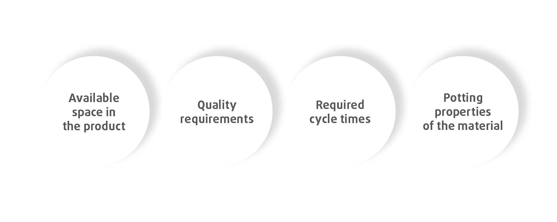
Figure 7: The size of the component must be considered for various reasons with regard to potting.
5. Define additional functions at an early stage
Sometimes components are completely potted, and there is no need for a cover. This simplifies the design and saves weight. Another benefit is that the potted components are shielded from view and therefore protected against industrial espionage (Fig. 8). Another form of potting is the sealing of components, for example to protect against environmental influences and corrosion. The objectives here are increased service life and functional reliability. Sensitive electronic surfaces, such as the surface of a printed circuit board, are coated with a thin layer of resin or protective varnish (Fig. 9).
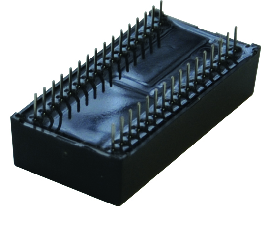
Figure 8: Potting to protect against industrial espionage is an additional function that is gaining in importance in high-tech industries.
In principle, potting surfaces can now be designed in such a way that they meet haptic requirements for end products. There is then no need for any housing. When designing components and products, however, the question always arises as to whether such properties are really needed, or whether a “cover solution” would not be the better option for repair purposes.
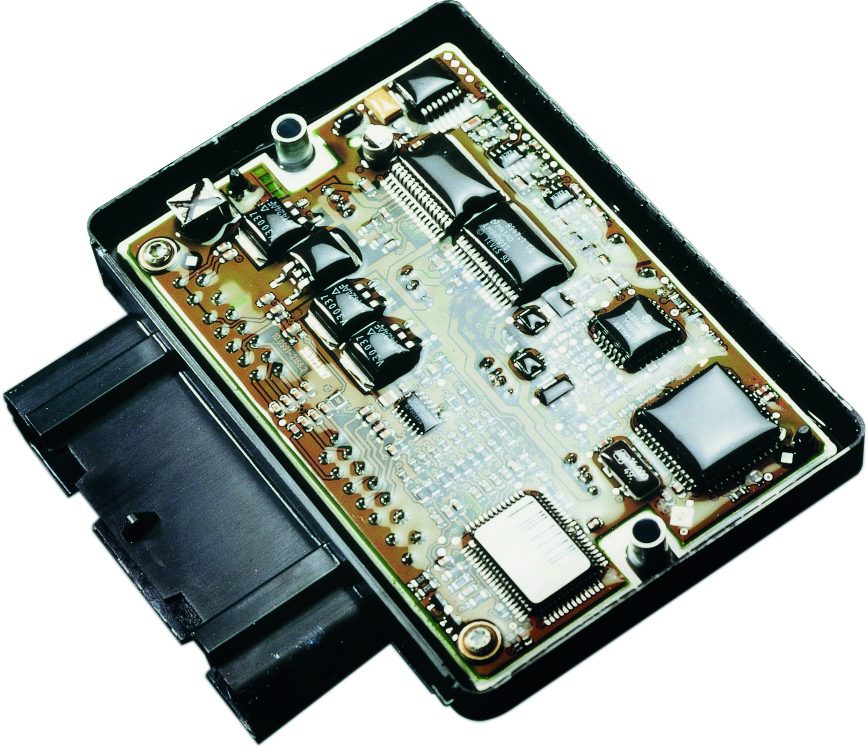
Figure 9: Sealing of a printed circuit board; make sure in this case that only the required areas are sealed.
Dispensing Solutions
In actual practice, there are cases where poor component design can no longer be changed. All that can then be done is to adapt the potting process. This means ensuring that the component is perfectly positioned under the dispensing needle so that potting compound reaches even the furthest corners of a component without bubbles and that all the air can escape. Depending on the potting system, there are various automation options here. They range from positioning solutions such as lifting and tilting units integrated in a three-axis system (Fig. 10) to robot arms (Fig. 11). Basically, the potting system needs to do more work, so cycle times are longer.
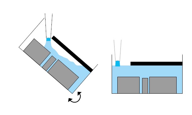
Figure 10: The component is first tilted so that the material fills the lower corner, and then moved to the horizontal position for the rest of the potting.
The resulting costs could have been avoided if the designers had liaised at an early stage with the production team or system supplier. In-house staff are usually fully trained on the available potting systems and have a lot of know-how. However, in view of dynamic developments in potting systems, experts working at the system suppliers have a better overview of new technologies. Consultation saves time and money in such cases.
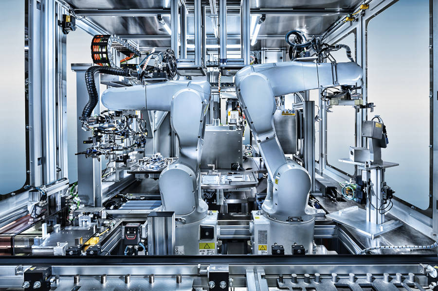
Figure 11: Robot solutions offer maximum flexibility in component positioning, but are usually the most expensive.
Consider Materials and Potting Technology
Material selection
The design and production teams not only develop the components, they also select the potting material. This must meet the product requirements and be appropriate for the component design. First of all, all the parties involved should be aware of the functions that the potting will be performing. Questions to be considered include the following:
- Does the component only need to be protected from moisture or mechanical stress?
- Are heat-conducting properties needed?
- Is insulation or dielectric strength required?
These questions are used to get material suppliers and system manufacturers on board in order to benefit from their experience and know-how, because every material behaves differently and therefore can be processed differently. This ultimately has an impact on what potting system is best for the job (automation, material preparation, dispensing, quality assurance, etc.).
There are many proven materials based on silicone, epoxy, or polyurethane that are available for effective protection of components (Fig. 12). Silicones, for example, have a surface that is excellent at repelling water. They are electrical insulators, dampen mechanical vibrations, and remain unchanged over a wide range of temperatures.
Polyurethanes are highly customizable. Depending on the formulation, they can be very soft or extremely hard after curing. These resins adhere very well to metals and shrink comparatively little during hardening. Their thermal conductivity is very good.
Epoxy resin has very good adhesive properties and excellent electrical insulation properties. Thermal resistance under continuous load is as high as 180 °C.
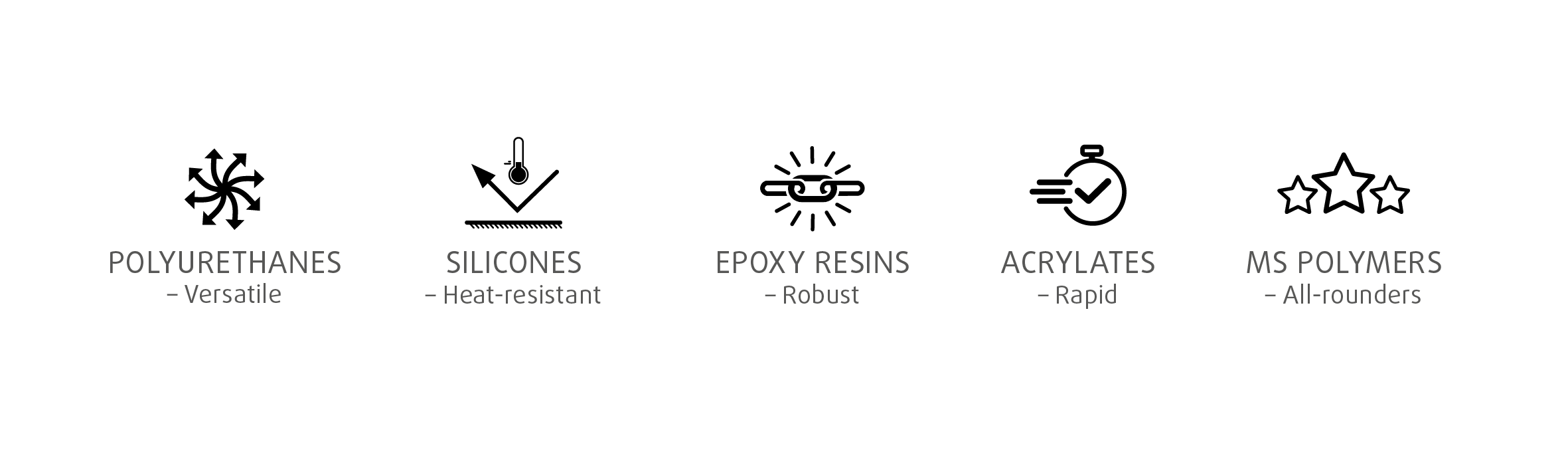
Figure 12: Each material has characteristic benefits but also places different requirements on the potting process.
Potting technology
Component design has a significant influence on whether potting should be under atmospheric pressure or under a vacuum. Vacuum potting is being increasingly used if potting has to be absolutely bubble-free to ensure, for example, high levels of functional quality, safety, and reliability for electronic components. Optimum design permits potting under atmospheric pressure up to a certain limit (very small dispensing spaces, undercuts, etc.) but sometimes only vacuum potting is the solution. In terms of the technologies, there are no restrictions. Proven solutions based on sophisticated process engineering are available today for both types of potting.
Validate Component Developments Early
Design security through testing
Design security comes from validating various aspects:
- How does the dispensing material flow through the component?
- Are planned design changes sufficient for absolutely bubble-free potting?
- Can potting under vacuum or potting with complex component positioning be avoided under certain circumstances?
Such questions are difficult to answer theoretically without sufficient experience. In such cases, testing in the Technology Center is recommended. These tests check the pottability of components under production conditions, providing an early indication of how a component can be optimized. The team also gets a clear idea whether the component design, material, and chosen potting technology work perfectly together. The Technology Center answers all relevant questions — at a time when any high follow-up costs can still be avoided. In terms of potting, the practical tests give manufacturers the assurance that they have fulfilled their responsibility to provide a functioning and durable component.
Optimize the Component Design Stage
Poor quality rejects and/or complaints due to faulty potting are expensive and — depending on the product — may damage the corporate image. Designers have a great influence on avoiding such problems from the outset. By adhering to the rules summarized in this white paper and by communicating at an early stage with all relevant stakeholders, they can make a huge contribution to achieving successful high-quality products. It makes sense to access know-how, experience, and services such as the technology centers of system and material suppliers at an early stage.
For more information, visit www.scheugenpflug-dispensing.com.
Images courtesy of Scheugenpflug GmbH.
Potting: https://www.adhesivesmag.com/keywords/2595-sealants-in-electricalelectronic
Potting process: https://www.adhesivesmag.com/keywords/2321-dispensing
Silicone: https://www.adhesivesmag.com/keywords/2368-silicones
Looking for a reprint of this article?
From high-res PDFs to custom plaques, order your copy today!


