Ink Jet Printing Adhesives
With the miniaturization of packaging in areas such as electronics, medical devices and wafer fabrication, spatially controlled, precise deposition of adhesives or adhesive-like materials into increasingly smaller spaces has become critically important. Ultraviolet- and electron beam-cured coatings, inks, and adhesives are essential materials for these advanced devices,1 and the need for higher-level packaging to increase board density and complexity also requires adhesive-specific technical advances.2
FUJIFILM Dimatix, a leading provider of commercial and industrial ink jet products, has developed a microdeposition ink jet technology that addresses this market demand for enhancing adhesive processes through non-contact patterned deposition. This past April, the company announced that its cartridge-based Dimatix Materials Printer (DMP) had been used to ink jet spatially controlled patterns of micron-sized adhesive drops. By printing such small and aligned drops, the ability to apply surface mount adhesives in tight junctions becomes both tractable and easy.
Printing Adhesives
Together with researchers in the Department of Biomedical Engineering at the University of North Carolina-Chapel Hill, FUJIFILM Dimatix researchers ink jetted monofunctional acrylate esters with proven repeatability. Using the DMP, the materials were printed onto glass slides and silicon wafers. Researchers printed patterns with 50 µm line widths - a significant advancement required for miniaturization.The DMP is a piezoelectric drop-on-demand ink jet printing tool that scientists and engineers can use to develop processes for depositing a variety of functional fluids. These fluids can be both Newtonian and non-Newtonian fluids, and contain polymers, nanoparticles, disordered particles, or mixtures. The base fluid can be organic or water-based with a range of viscosities.
For this particular application, not only is the jettability of a large range of viscosities important, but the ability to control the temperature during deposition is as well. The DMP has temperature control in the printhead to 3°C. A thermistor controls this narrow temperature range, thereby minimizing temperature-dependent viscosity effects.
The DMP is based on a cartridge printhead system, wherein fluid is injected into the fluid module, which is then snapped to the jetting module to form a sealed cartridge. The ink jet printhead itself is a silicon structure consisting of 16 individually addressable jets, an array of inline nozzles that are spaced 254 µm apart. The effective nozzle diameter is 21.5 µm, which provides droplets in the ~10 pL range. The printhead is powered by a thin piezoelectric unimorph, and actuation occurs in the plane of the wafer.
The DMP has a preloaded waveform that has been optimized for fluids with viscosities of 10-12 centipoise (cps) and surface tensions of 28-33 dynes/cm. This waveform can be changed in pulse shape (amplitude, slew rate and duration), frequency, and voltage, as may be required for new fluids. The waveform has two segments - a jetting segment and a non-jetting segment. The jetting segment is usually the segment that is manipulated the most to jet non-optimized fluids (those with viscosities above or below 10-12 cps and surface tensions above or below 28-33 dynes/cm). If waveform parameters are modified systematically, fluids that are challenging to jet may be deposited successfully.
With the DMP, patterning of lines or figures can be accomplished using Gerber images, bitmap images or a pattern generator in the software. In this case, the researchers used the Dimatix Drop Manager software pattern generator to generate a dot matrix.
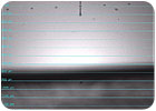
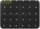
The DMP's fiducial camera was used for optical microscopy after printing. Figure 1 shows the drop formation of the monofunctional acrylate ester at the nozzle plate as the drop is exiting from an individual nozzle. Figure 2 shows an optical micrograph of the resulting drop pattern onto the silicon wafer. The resulting drops were approximately 56 µm each, and spacing between drops was approximately 266 µm. The monofunctional acrylate ester was used "as manufactured," indicating the ease of use of the DMP.

MEMS-Based Ink Jet Technology
FUJIFILM Dimatix's piezoelectric ink jetting technology and MEMS fabrication processes are the backbone of the DMP. Unlike thermal ink jet technology, which uses tiny resistors to heat and vaporize ink to create a bubble that expands to push ink out of a nozzle, piezoelectric technology uses mechanical deformation to create acoustic vibrations that force ink out of a nozzle and pull more ink into the reservoir to replace the ink that has been jetted out.Commercialized in the early 1990s, MEMS technology was originally used to create miniature mechanical devices such as fluid, pressure, temperature, and vibration sensors and valves. MEMS technology has moved beyond its semiconductor manufacturing-based roots to include many other applications, including fabricating ink jet printheads with precisely defined architectures.
The miniature scale of MEMS lends itself to the creation of tightly packed and highly integrated structures that can jet ink drops an order of magnitude smaller than previously possible. Further, the mechanically robust and chemically inert nature of silicon provides an extremely durable material that is impervious to most fluid chemistries.
Ink Jet Printing Vs. Other Dispensing Technologies
Generally, most adhesive-like materials are deposited using pin transfer, screen printing or stencil printing. These methods can be used to place drops of both conductive and non-conductive adhesives with various chemical and physical properties.Stenciling is one available technology for the patterning of adhesives, however there are several disadvantages to the process. First, the typical dip and stamp setup requires excessive amounts of adhesive material. Additionally, there is no control of individual adhesive drop placement or volume. Also, stencils wear out over time, so deposition precision decreases with each stamping event. Ink jet printing can overcome these limitations.
In pin transfer, a series of pins matching the required surface-mount adhesive pattern is dipped into an adhesive fluid. The pins then make physical contact with the substrate, allowing transfer of the adhesive to the circuit board. Any time a circuit board pattern is changed, a new pin tool has to be produced. In addition, the adhesive fluid container has to be large enough for each pin to be simultaneously dipped in the adhesive, meaning that restricting exposure to the physical and chemical environment of the holding tray becomes paramount due to its large surface area. Pin transfer is also difficult for patterns smaller than a 3216 chip resistor,3 which is a land pattern of an area width of 1.2 mm. This becomes a process limitation as circuit boards become more populated and concomitantly decrease in size.
In contrast, the DMP has highly accurate drop placement with drop sizes around 40 µm. The DMP can accurately place 900 drops in the same place to target the same 3216 adhesive area. If the area shrinks, the only change necessary is in the pattern printed.
In screen-printing adhesives, a screen with the correct pattern for the adhesive is put over the circuit board, and then the adhesive is applied by squeegee through the holes. Like pin transfer, the adhesive fluid is in an air-containing environment. The presence of air may alter the chemical properties of the adhesive. In contrast, the DMP keeps the fluid contained in a closed chemical environment, so there is no exposure to air during the printing process.
Implications
Microscopic deposition of adhesives enables improved bonding for a range of advanced electronic and biomedical applications. By printing such small and spatially aligned drops, bond lines between materials are reduced, ultimately resulting in increased bond strength and structural integrity.Using ink jet printing to dispense adhesives has implications for a variety of industries in myriad current and future applications. In addition to electronics packaging and wafer fabrication, there are also opportunities in the biomedical field. For example, researchers are ink jetting adhesives in a quest for a bio-based composite for surgical applications.
To best leverage ink jet technology for depositing adhesives, the adhesives must be formulated correctly. With advances in adhesive materials - like the development of new hybrid materials (such as those having properties of both glue and a conductor) - both dual and multifunctional materials can be deposited in gap junctions. Ink jet printing can help researchers precisely deposit small amounts of adhesives for optimal results.
For more information on ink jetting technology, contact FUJIFILM Dimatix Inc., 2230 Martin Avenue Santa Clara, CA 95050; phone (888) 346-2849 or (408) 565-9150; fax (408) 565-9151; e-mail info@dimatix.com ; or visit http://www.dimatix.com .
SIDEBAR: Printing Adhesives for Sensors
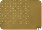
As part of a grant from the National Institutes of Health (NIH), a research team in the Department of Biomedical Engineering at the University of North Carolina-Chapel Hill is conducting novel research in the area of biomedical sensors. Anand Doraiswamy, M.S., and Associate Professor Roger Narayan, M.D. Ph.D., are looking at new materials and methods for creating effective cell-based sensors for a variety of applications, including drug discovery and pathogen detection.The team has been successful in repeatedly depositing precise, spatially aligned microscale cyanoacrylate adhesive patterns with resolutions of 25 µm on a variety of substrates using the Dimatix Materials Printer (DMP). Since the DMP dispensing process is not heat-based, researchers can print adhesives "as is," keeping adhesive properties intact with no loss to bonding strength.
Based on initial findings, the team aims to demonstrate an actual device based on attaching agents to the adhesives. The idea is that once the adhesive is patterned on a microarray, living cells and other sensor materials can be deposited precisely on top of the adhesive patterns. The result would be cell-based sensors that bond to the substrate with no need for chemical modification or combination with a bonding solvent. These cell-based sensors may be effective in the detection of bacteria, fungi, viruses, or other biological agents.
Links
Looking for a reprint of this article?
From high-res PDFs to custom plaques, order your copy today!


